Ah. Good. Questions. I was ready to go of into my next spiel.
More quantitative answers in what would be the optimal number of registers will come later (there are some fancy techniques of register renaming, and other compiler assisted things that can be done).
The short answer is that the processor will have as many registers as the designer deemed fit. It is a finite number, but in many designs can be made to look "infinite for practical purposes."
Keep in mind that very few people actually write assembly code directly. Compilers have some neat ways of assigning registers to variables used in a higher level program like C. Depending on how long people want to stay with my explanations, we may get to that.
I did go through that part pretty quickly. The processor is a piece of hardware. It is in-fact usually a very big integrated circuit built on silicon (usually though GaAs other substrates may be used).
All it does is process information. It needs to "communicate" to the other devices it is hooked-up to. Whether that is a motor-controller, a hard-disk controller, a USB hub, or a graphics card, the programmer usually specifies the communications as reads/writes to I/O ports and/or memory-mapped I/O.
"Memory-mapped I/O" is just a way of saying that particular addresses in "memory" are actually not memory, but I/O ports in disguise. They aren't actually memory locations, they just look look like memory to the programmer.
Hopefully, things will become clearer as we go.
Memory (Random Access Memory), is usually "remembered" till the power is shut-off. This type of memory is called volatile memory. Flash, EEPROM, and other such things keep the bits written to them even when it gets no power, and is referred to as non-volatile memory.
Things will become slightly more concrete. However, as they become concrete, it will also become technical. Computer arithmetic(in a nutshell), and how execution works (at a high level) was going to be next brain-dump.
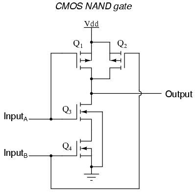
Yes. A processor is a circuit itself. It is connected electrically through "wires" (Printed Circuit Board, and package "traces") to other circuits.
When a programmer specifies writes/reads to I/O ports, this creates "traffic" ("signals" toggling on the "wires") following specific protocols (PCI, ATA, USB, etc. are protocols) that communicates to other circuits (note that these circuits could in turn communicate with other circuits used to control your monitor, your modem, and other things).
No problem.
Like I mentioned elsewhere, I suddenly got the overwhelming urge to explain stuff. I don't know why.
But believe me, it is my pleasure.
User Tag List
View Poll Results: So Please Choose:
- Voters
- 22. You may not vote on this poll
-
08-23-2008, 01:27 AM #11
Accept the past. Live for the present. Look forward to the future.
Robot Fusion
"As our island of knowledge grows, so does the shore of our ignorance." John Wheeler
"[A] scientist looking at nonscientific problems is just as dumb as the next guy." Richard Feynman
"[P]etabytes of [] data is not the same thing as understanding emergent mechanisms and structures." Jim Crutchfield
-
08-23-2008, 01:30 AM #12
Ah, very nice! I'll save some questions which are already springing to mind for your upcoming posts....
Madman's azure lie: a zen miasma ruled.
Realize us, Madman!
I razed a slum, Amen.
...............................................
-
08-23-2008, 03:35 AM #13
A good place to start on the next part is a bit difficult. Striking the proper level of abstraction is harder than I thought.
Real processors would have much more sophisticated, ISAs and machine models. There is also an issue with Big Endian vs. little endian, stack-pointers, segments, etc. that I am excluding from this model.
But, for illustration purposes, lets say our Instruction Set Architecture (ISA) is the following (completely made up and rather impractical):
opcode 0x0: HALT # halts the processor
opcode 0x1: BNZ <register> <label> # Branch to <label> if the value in <register> is not 0
opcode 0x2: ADD <register1> <register2> # Add the value of <register2> to <register1> and store the result in <register1> (old value lost)
opcode 0x3: SUB <register1> <register2> # Subtract the value of <register2> to <register1> and store the result in <register1> (old value lost)
opcode 0x4: AND <register1> <register2> # And the value of <register2> to <register1> and store the result in <register1> (old value lost)
opcode 0x5: OR <register1> <register2> # And the value of <register2> to <register1> and store the result in <register1> (old value lost)
opcode 0x6: SHL <register> <constant> # shift the value in <register> by <constant> (between 0 and 8) for this instruction.
opcode 0x7: ROR <register> <constant> # rotate the value in <register> by <constant> (between 0 and 8) for this instruction.
opcode 0x8: LDC <register> <constant> # load <constant> (0 to 255) into <register>
opcode 0x9: RDM <register1> (<register2>) #read the value stored at the address denoted by the value stored in <register2> to <register1>
opcode 0xA: WRM (<register1>) <register2> #write the value in <register1> into the location specified by the address in <register2>
opcode 0xB: IN <register> <port> # read a port
opcode 0xC: OUT <port> <register> # write a port
Note: 4-bit opcode used for each instruction.
So the instruction format is a 20-bit format:
4-bits opcode, followed by 8-bit operand 1, followed by 8-bit operand 2.
We have the following general registers:
A,B, C, D (make them all 8-bit registers for now).
Register Codes (2-bits):
A:0x0, B:0x1, C:0x2, D:0x3
When a register is an operand, only the 2 least significant bits are used.
Lets say you have 2 I/O ports:
IO_A (port code 0) is an 8-bit port where if you write there, two 7-segment LEDs will display the value written in hexadecimal. When you read that port, you will get back the last value you wrote. On Power-on, that port will initialize to 0x00 (hexadecimal for all 8-bits being 0)
IO_B (port code 1) is another 8-bit port hooked up to 8 2-pole on-off switches (numbered 7 down to 0). When you read this port, you get back a binary value (which we will generally short-hand use hexadecimal values) representing which switches are on. Getting back 0x01 means switch 0 is on, and all the rest are off. Getting back 0x02 means switch 1 is on, and the rest are off. Getting back 0x03 means switches 1 and 0 are on, and all the rest are off. ... Writing this port does nothing.
When a register is an operand, only the least significant bits are used.
Lets say you can address 2^8=256 memory locations (all "well-behaved," i.e. not memory-mapped I/O). Lets further say that this space is only available for "data" that your programs will read and write from and to.
Lets pretend there is is this magical "code space" where all the instructions of you program sits, and you can program this space with an external programmer.
Once the external programmer is done, it resets a special purpose register called the "Program Counter" to 0. All your programs are placed in code-space with the first instruction at 0. Lets assume that an 8-bit Program counter is enough.
Believe it or not that is about as simple as I could make the model anticipating the type of stuff I want to include in the next few brain-dumps.
Now lets translate the some Assembly to machine code.
The Assembler Code will cause memory locations 0x0 through 0xA to have the values 0x0 through 0xA, and the 7-segment display to count down from 0xA to 0x0:
LDC A 0xB
LDC B 1
L1:SUB A B
WRM (A) A
OUT IO_A A
BNZ A L1
HALT
Machine Code:
0:0x8000B
1:0x80101
2:0x30001
3:0xA0000
4:0xC0000
5:0x10002
6:0x00000
Lets see if you understood this (completely made-up) machine model and the example translation (hopefully I didn't make mistakes). If so, I can walk you through what happens to the registers, memory and ports, step by step.
Accept the past. Live for the present. Look forward to the future.
Robot Fusion
"As our island of knowledge grows, so does the shore of our ignorance." John Wheeler
"[A] scientist looking at nonscientific problems is just as dumb as the next guy." Richard Feynman
"[P]etabytes of [] data is not the same thing as understanding emergent mechanisms and structures." Jim Crutchfield
-
08-23-2008, 01:02 PM #14
I get the gist of it. Feel free to continue.
-
08-23-2008, 03:55 PM #15
OK, so the programmer loads the following program into code-space:
0:0x8000B
1:0x80101
2:0x30001
3:0xA0000
4:0xC0000
5:0x10002
6:0x00000
This is the state of the registers (U=unknown):
PC:0x00
A :0xUU
B :0xUU
C :0xUU
D :0xUU
All the memory locations have unknown values, the 7-segment display is showing some random hex value, and the switches are irrelevant for this program.
All processors go through a cycle similar to the following:
1) Fetches the next instruction
2) Decodes the instruction
3) Executes the instruction
Modern machine are quite a bit more complicated in that they often fetch many instructions at a time use branch-prediction, often have multiple pipelines at various stages of execution, and have to have a way to "retire" the instructions in the correct order, but we'll stick to the simple version for a while.
First cycle:
Fetches, the following:
0:0x8000B
Decodes it to mean
Load Constant 0x0B into register 0 (i.e. Register A)
It then executes the instruction, yielding:
A :0x0B
Since the instruction was not a branch instruction, it auto-updates the PC.
PC : 0x01
Second cycle:
Fetches, the following:
1:0x80101
Decodes it to mean
Load Constant 0x01 into register 1 (i.e. Register B)
It then executes the instruction, yielding:
B :0x01
Since the instruction was not a branch instruction, it auto-updates the PC.
PC : 0x02
Third cycle:
Fetches, the following:
2:0x30001
Decodes it to mean
Subtract the value in register 1 (register B) from register 0 (Register A), and keep result in Register 0.
It then executes the instruction, yielding:
A :0x0A
Since the instruction was not a branch instruction, it auto-updates the PC.
PC : 0x03
Fourth cycle:
Fetches, the following:
3:0xA0000
Decodes it to mean:
Write memory addressed by register 0 (register A) the value in register 0 (Register A).
It then executes the instruction, yielding a change in memory location 0x0A:
0x0A :0x0A
Since the instruction was not a branch instruction, it auto-updates the PC.
PC : 0x04
Fifth cycle:
Fetches, the following:
4:0xC0000
Decodes it to mean:
Decodes it to mean output to port 0 (port IO_A) the value in register 0 (Register A).
It then executes the instruction, yielding a change to the seven segment display:
0x0A is displayed on the pair of 7-segment displays.
Since the instruction was not a branch instruction, it auto-updates the PC.
PC : 0x05
6th cycle:
Fetches, the following:
5:0x10002
Decodes it to mean:
If the value in register 0 (register A) is not zero, change the program counter to 0x02
It then executes the instruction:
Since the value in the register A is 0xA (therefore not zero), the program counter is changed.
PC:0x02
7th cycle:
Fetches, the following:
2:0x30001
Decodes it to mean
Subtract the value in register 1 (register B) from register 0 (Register A), and keep result in Register 0.
It then executes the instruction, yielding:
A :0x09
Since the instruction was not a branch instruction, it auto-updates the PC.
PC : 0x03
Note that this is the same as the 3rd cycle except the values are changed. The Eight through 10th are essentially repeats of 4rth through 10th as well. It will keep looping from PC value 0x02 through 0x05, that is till ...
46th cycle:
Fetches, the following:
5:0x10002
Decodes it to mean:
If the value in register 0 (register A) is not zero, change the program counter to 0x02
It then executes the instruction:
Since the value in the register A is 0x0, the program counter proceeds with its normal auto-update.
PC:0x06
47th cycle:
Fetches, the following:
6:0x00000
Decodes it to mean:
Halt the processor.
It then executes the instruction:
The processor execution is stopped.
Hopefully, the actual execution makes sense because, next, I plan to give some insight into the circuits that actually make this happen.
Also, if the pace is too slow, let me know. We haven't really gotten to the point at which we are talking about the types of decisions Computer (Micro-)Architects have to make. There is a lot of back-ground information needed.
Accept the past. Live for the present. Look forward to the future.
Robot Fusion
"As our island of knowledge grows, so does the shore of our ignorance." John Wheeler
"[A] scientist looking at nonscientific problems is just as dumb as the next guy." Richard Feynman
"[P]etabytes of [] data is not the same thing as understanding emergent mechanisms and structures." Jim Crutchfield
-
08-23-2008, 04:11 PM #16
-
08-24-2008, 12:42 AM #17
OK. Either people have lost interest or there or no questions. I was expecting there to be some before I came back. Anyway, I'll do a short dump before I sign off.
I will be really surprised if there aren't questions after this, because we ought to be close to an implementable design of a microprocessor (an impractical one, though it may be) if I did things right. Note that this is a very crude implementation, more thought and care would be needed to make an optimal micro-architecture of the machine model presented earlier.
I'll include an attachment showing the block diagram of our little toy processor. (Note:I used a crude OpenOffice Draw package to do this, so the symbols are not standard)
There are going to be four blocks that are "clocked" by our cycle-clock, the Program Counter (PC), the memory, the register bank, and the ports. These four banks are indicated by those squiggly lines feeding them. What this means is that these blocks will hold on to their old values, till the next rising edge of our cycle clock, the they will accept the new values being fed to them.
The Code Space in our processor is clocked by the external programmer, and not the main cycle-clock.
The other two blocks are "logic" blocks, that don't have clocked elements. Based on the way I am using the buses (described soon), the fetch is trivial, and the decode is fairly straightforward also. The execute however does the brunt of the work, and may require a lot of explanation in a separate brain dump of its own.
Note, that the arrows in the diagram are "buses" or communication channels between the blocks.
The buses for the Memory, Ports and Registers, have three parts each. Each have an Address/Control Bus, a Read Data Bus, and a Write Data Bus. The Address/Control Buses are comprised of their respective addresses and more bits to indicate which are target and which are source (some are both). The Data Buses are as wide as to accommodate the most sources going to the Execute logic, and the targets coming from the execute unit.
We can view the Current PC as an "address" to the Code Space, and the instructions as the "data" coming from the code space.
So to Summarize the Buses:
Current PC Bus - 8-bits
New PC Bus- 8-bits
Instruction Bus- 20-bits
Port Address/Control (PAC) Bus - 3-bits, 1-bit port address, 1-bit indicating that it is source, 1-bit indicating that its target
Port Read Data (PRD) Bus - 8-bits
Port Write Data (PWD) Bus - 8-bits
Register Address/Control (RAC) Bus - 9-bits, two 2-bit register address, 2-bit indicating source, 1-bit indicating target
Register Read Data (RRD) Bus - 16-bits (2 8-bit source data potentially)
Register Write Data (RWD) Bus - 8-bits
Op.Code+Constant Bus - 12-bit, 4 bit opcode + 8-bit constant
Data-bus - for intermediate data, 8-bits
Now I am going to leave it up to questions (because I know there ought to be), before I explain further, to make sure I am not just being futile by posting.Last edited by ygolo; 08-24-2008 at 08:17 PM.
Accept the past. Live for the present. Look forward to the future.
Robot Fusion
"As our island of knowledge grows, so does the shore of our ignorance." John Wheeler
"[A] scientist looking at nonscientific problems is just as dumb as the next guy." Richard Feynman
"[P]etabytes of [] data is not the same thing as understanding emergent mechanisms and structures." Jim Crutchfield
-
08-24-2008, 02:21 AM #18
I have some questions (turns out the gist just wasn't enough).
-Translating from assembly code to machine code.-
I'm not 100% sure of what's going on there (I thought I did, but I decided to test myself...and I failed). Could you give a step-by-step explanation of the process?
-Processor cycle thing.-
Why does the looping happen? Why do things become different at cycle 46?
-Miscellaneous-
What is "clocking" or "clocked"?
What exactly are bits, and why have you labeled several things (buses, opcodes, etc) with something like "x bits"?
Could you give a brief tutorial (or something) on hexadecimal?
------------------------------------------------------------------------------
And lastly, I have a suggestion:
Start off posts with definitions of technical terms that you'll be using in the post, and that a layman might not be familiar with.
-
08-24-2008, 06:44 AM #19
I am not entirely thinking straight right now, but hopefully coherent enough to answer your questions. I'm not sure when I'll wake up and am sure I'll have a headache when I do.
I'll start with hexadecimal (and cover "bit" along with it).
Hexadecimal is base sixteen, with the decimal numbers used for 0 through 9, and...
A=10, B=11, C=12, D=13, E=14, F=15.
Computers do all their math (and most of their other work) in base 2. Each place value in base 2 is a "bit" or binary digit. These bits are transfered/stored in forms that only require two different levels/modes/states/whatever. This small number of states is what makes bit so attractive for computing. When I say something is 4 bits, I mean it uses/stores/transfers/whatever 4 binary-digits.
Without having fonts installed, using subscripts on a computer is not possible. So we denote all hexadecimal number with a "0x" or "'h" prefix, or an "h" suffix. "0x" is most popular (especially in software). The tick notation is used in Verilog HDL (Hardware Description Language) (Verilog is currently the most popular HDL in the U.S., and should not be confused with VHDL which is another language popular in Europe).
The reason we use hexadecimal is that it works really easily when wanting to convert to base 2. Base ten would require various calculations not required in base 16. Note that each place value (often called a "nibble" by Computer Engineers) in base-16 is equivalent to exactly 4 place values in base 2.
There are two "nibbles" in a "byte" (8-bits), get it?
Binary values are often denoted with a "'b" prefix. So 'b0101=0x5=5 (in base 10). In verilog, the constant value actually has the number of bits prefixed to the constant, so you'd see 4'b0101 in the code itself. Sorry, I'm rambling...
The conversion between base 2 and base 16 (other than the normal way) involves simply memorizing 16 translations.
Here is the full translation:
0=0x0='b0000
1=0x1='b0001
2=0x2='b0010
3=0x3='b0011
4=0x4='b0100
5=0x5='b0101
6=0x6='b0110
7=0x7='b0111
8=0x8='b1000
9=0x9='b1001
10=0xA='b1010
11=0xB='b1011
12=0xC='b1100
13=0xD='b1101
14=0xE='b1110
15=0xF='b1111
Now, if you want to interpret hexadecimal number 0xBADCAD into binary you'd simply replace each nibble with its appropriate four bit translation.
In this case:
0xBADCAD='b1011 1010 1101 1100 1010 1101 (spaces used to keep the nibbles visible)
Also, (although conventions differ) in any base, the left most bit/digit/hex-"nibble," is "most significant" (i.e. has the highest place value), while the right most bit/ digit/hex-nibble is "least significant" (i.e. has the least place value).
Going from binary to hexadecimal, we often don't have enough bits for a nibble, so we pad the most significant bits with zeros. So 'b10='b0010=0x2.
Now to the machine code translation...
I made the machine code really stripped down, so many of the complications in real machines are not here. It was meant for illustration purposes, but I plan to keep using it, so I should make things clear here.
I'll do the subtraction line for illustration.
L1:SUB A B
Note the label L1, in our case is irrelevant for this instruction, it is just a way for the BNZ instruction before the HALT to know where to "branch" to. So we're left with:
"SUB A B" which denotes opcode 0x3, register 0x0 for the first operand, and register 0x1for the second operand. Note that the register codes for the operands are only 2 bits each, so they are padded with zeros in the 6 most significant bits. We get opcode 0x3, operand code 0x00, and operand code 0x01. Put them together, and we get 0x30001.
Ah, branching...
So there is the special instruction in our ISA denoted "BNZ" which stands for "branch if not zero." This checks the prescribed register to see if it is not zero. If it is not zero, then it changes the PC to where the label in that instruction specified.
In our case, the label was L1, which was the SUB instruction mentioned earlier, sitting in the third slot of code space (slot 0x2). If the register specified is zero, we move on to the instruction immediately following it in code space.
Clocks are a means for all the circuits in a processor (and many other digital circuits as well) to synchronize with each other. It is a periodically repeating signal. The most common implementation is signal that switches between a high-voltage level and a low-voltage level and vise-versa at regular intervals. When I say "rising edge" of a clock, I mean the transition from the low-voltage to the high-voltage.
I'll keep that in mind. I have been doing computing stuff since I was 13, and have worked professionally in some capacity (software engineer, systems engineer, or component engineer) since I was 18, so sometimes I have no perspective on what a layperson would know. Also, many computing terms are hard to define, and many are newly minted. I once used the terms "clauses, and qualifiers" (based on some precedent from other designs) and those words made their way into becoming regular terms used by people working on many chips, and is even going to be in a protocol spec. to be released. nVidia uses the term "warp" to describe something very similar to "thread" in the vernacular of most computer folks, and use the word "thread" for something else funky but similar.
Please, go through the last few posts, and keep asking questions. There is a lot of arbitrariness in computing. Sometimes, you won't understand something till you know the convention (and the convention is easy to assume for someone who uses it regularly).
Hopefully, this made sense to you (or at least will to me in the morning). Please keep asking questions for clarification.
It may seem like I didn't cover much ground, but what I posted is only a few steps away from all the info. needed to design a crude processor like the one described.
So again, please keep asking questions for clarifications.
Accept the past. Live for the present. Look forward to the future.
Robot Fusion
"As our island of knowledge grows, so does the shore of our ignorance." John Wheeler
"[A] scientist looking at nonscientific problems is just as dumb as the next guy." Richard Feynman
"[P]etabytes of [] data is not the same thing as understanding emergent mechanisms and structures." Jim Crutchfield
-
08-24-2008, 12:15 PM #20
I'm back on track. I say move on...
Thanks for doing this, by the way. Computer architecture is interesting stuff.
Similar Threads
-
For those born in October: What type are you?
By hommefatal in forum The Fluff ZoneReplies: 5Last Post: 06-12-2009, 02:01 PM -
Prayers by the Lake - for those interested in Eastern Christian mysticism
By Sniffles in forum Philosophy and SpiritualityReplies: 31Last Post: 12-02-2008, 04:51 PM -
For those who believe in spirit/soul...
By Little Linguist in forum Philosophy and SpiritualityReplies: 40Last Post: 08-16-2008, 09:17 AM